- 您现在的位置:买卖IC网 > Sheet目录3881 > PIC18F8520T-E/PT (Microchip Technology)IC PIC MCU FLASH 16KX16 80TQFP
2004 Microchip Technology Inc.
DS39609B-page 105
PIC18F6520/8520/6620/8620/6720/8720
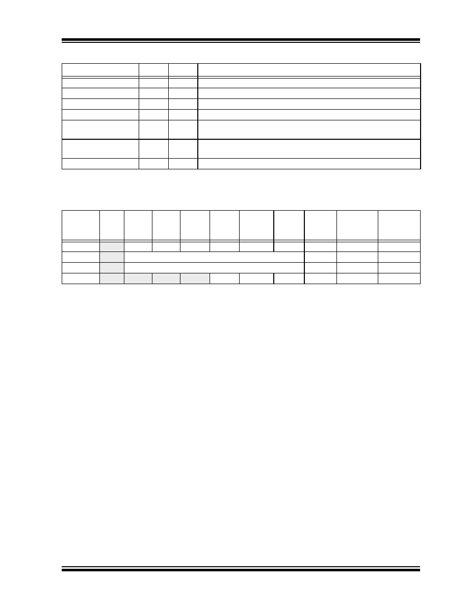
TABLE 10-1:
PORTA FUNCTIONS
TABLE 10-2:
SUMMARY OF REGISTERS ASSOCIATED WITH PORTA
Name
Bit#
Buffer
Function
RA0/AN0
bit 0
TTL
Input/output or analog input.
RA1/AN1
bit 1
TTL
Input/output or analog input.
RA2/AN2/VREF-
bit 2
TTL
Input/output or analog input or VREF-.
RA3/AN3/VREF+
bit 3
TTL
Input/output or analog input or VREF+.
RA4/T0CKI
bit 4
ST
Input/output or external clock input for Timer0.
Output is open-drain type.
RA5/AN4/LVDIN
bit 5
TTL
Input/output or slave select input for synchronous serial port or analog
input, or Low-Voltage Detect input.
OSC2/CLKO/RA6
bit 6
TTL
OSC2 or clock output, or I/O pin.
Legend: TTL = TTL input, ST = Schmitt Trigger input
Name
Bit 7
Bit 6
Bit 5
Bit 4
Bit 3
Bit 2
Bit 1
Bit 0
Value on
POR, BOR
Value on
all other
Resets
PORTA
—
RA6
RA5
RA4
RA3
RA2
RA1
RA0
-x0x 0000 -u0u 0000
LATA
—
LATA Data Output Register
-xxx xxxx -uuu uuuu
TRISA
—
PORTA Data Direction Register
-111 1111 -111 1111
ADCON1
—
VCFG1 VCFG0
PCFG3
PCFG2
PCFG1
PCFG0
--00 0000 --00 0000
Legend: x = unknown, u = unchanged, – = unimplemented locations read as ‘0’.
Shaded cells are not used by PORTA.
发布紧急采购,3分钟左右您将得到回复。
相关PDF资料
XF2J-2624-11
CONN FPC 26POS 0.5MM SMT
PIC18F8585T-I/PT
IC PIC MCU FLASH 24KX16 80TQFP
XF2J-2424-11
CONN FPC 24POS 0.5MM SMT
PIC18LF6585T-I/PT
IC PIC MCU FLASH 24KX16 64TQFP
PIC18LF6680T-I/PT
IC PIC MCU FLASH 32KX16 64TQFP
XF2J-2224-11
CONN FPC 22POS 0.5MM SMT
PIC18F6525T-I/PT
IC PIC MCU FLASH 24KX16 64TQFP
PIC18F4439-E/ML
IC PIC MCU FLASH 6KX16 44QFN
相关代理商/技术参数
PIC18F8520T-I/PT
功能描述:8位微控制器 -MCU 32KB 2048 RAM 68I/O RoHS:否 制造商:Silicon Labs 核心:8051 处理器系列:C8051F39x 数据总线宽度:8 bit 最大时钟频率:50 MHz 程序存储器大小:16 KB 数据 RAM 大小:1 KB 片上 ADC:Yes 工作电源电压:1.8 V to 3.6 V 工作温度范围:- 40 C to + 105 C 封装 / 箱体:QFN-20 安装风格:SMD/SMT
PIC18F8520T-I/PTG
功能描述:8位微控制器 -MCU 32KB 2048 RAM 68I/O Lead Free Package RoHS:否 制造商:Silicon Labs 核心:8051 处理器系列:C8051F39x 数据总线宽度:8 bit 最大时钟频率:50 MHz 程序存储器大小:16 KB 数据 RAM 大小:1 KB 片上 ADC:Yes 工作电源电压:1.8 V to 3.6 V 工作温度范围:- 40 C to + 105 C 封装 / 箱体:QFN-20 安装风格:SMD/SMT
PIC18F8525-E/PT
功能描述:8位微控制器 -MCU 48KB 3840 RAM 68I/O RoHS:否 制造商:Silicon Labs 核心:8051 处理器系列:C8051F39x 数据总线宽度:8 bit 最大时钟频率:50 MHz 程序存储器大小:16 KB 数据 RAM 大小:1 KB 片上 ADC:Yes 工作电源电压:1.8 V to 3.6 V 工作温度范围:- 40 C to + 105 C 封装 / 箱体:QFN-20 安装风格:SMD/SMT
PIC18F8525-I/PT
功能描述:8位微控制器 -MCU 48KB 3840 RAM 68I/O RoHS:否 制造商:Silicon Labs 核心:8051 处理器系列:C8051F39x 数据总线宽度:8 bit 最大时钟频率:50 MHz 程序存储器大小:16 KB 数据 RAM 大小:1 KB 片上 ADC:Yes 工作电源电压:1.8 V to 3.6 V 工作温度范围:- 40 C to + 105 C 封装 / 箱体:QFN-20 安装风格:SMD/SMT
PIC18F8525T-I/PT
功能描述:8位微控制器 -MCU 48KB 3840 RAM 68I/O RoHS:否 制造商:Silicon Labs 核心:8051 处理器系列:C8051F39x 数据总线宽度:8 bit 最大时钟频率:50 MHz 程序存储器大小:16 KB 数据 RAM 大小:1 KB 片上 ADC:Yes 工作电源电压:1.8 V to 3.6 V 工作温度范围:- 40 C to + 105 C 封装 / 箱体:QFN-20 安装风格:SMD/SMT
PIC18F8527-I/PT
功能描述:8位微控制器 -MCU 48 KB 4K RAM 70 I/O RoHS:否 制造商:Silicon Labs 核心:8051 处理器系列:C8051F39x 数据总线宽度:8 bit 最大时钟频率:50 MHz 程序存储器大小:16 KB 数据 RAM 大小:1 KB 片上 ADC:Yes 工作电源电压:1.8 V to 3.6 V 工作温度范围:- 40 C to + 105 C 封装 / 箱体:QFN-20 安装风格:SMD/SMT
PIC18F8527T-I/PT
功能描述:8位微控制器 -MCU 48 KB 4K RAM 70 I/O RoHS:否 制造商:Silicon Labs 核心:8051 处理器系列:C8051F39x 数据总线宽度:8 bit 最大时钟频率:50 MHz 程序存储器大小:16 KB 数据 RAM 大小:1 KB 片上 ADC:Yes 工作电源电压:1.8 V to 3.6 V 工作温度范围:- 40 C to + 105 C 封装 / 箱体:QFN-20 安装风格:SMD/SMT
PIC18F8585-E/PT
功能描述:8位微控制器 -MCU 48KB 3328 RAM 68I/O RoHS:否 制造商:Silicon Labs 核心:8051 处理器系列:C8051F39x 数据总线宽度:8 bit 最大时钟频率:50 MHz 程序存储器大小:16 KB 数据 RAM 大小:1 KB 片上 ADC:Yes 工作电源电压:1.8 V to 3.6 V 工作温度范围:- 40 C to + 105 C 封装 / 箱体:QFN-20 安装风格:SMD/SMT